Joan and Irwin Jacobs Announce $133-Million Naming Gift for the Technion-Cornell Innovation Institute

16The Joan and Irwin Jacobs Technion-Cornell Innovation Institute is a key component of Cornell Tech in New York City; program will offer unique dual master’s degrees

NEW YORK – Dr. Irwin Mark Jacobs, Founding Chairman and CEO Emeritus of Qualcomm, and his wife Joan Klein Jacobs, today announced a $133-million gift to Cornell University and the Technion-Israel Institute of Technology to create the Joan and Irwin Jacobs Technion-Cornell Innovation Institute (JTCII). The JTCII is a key component of Cornell Tech, whose permanent campus will be located on Roosevelt Island. The funds will help support curriculum initiatives, faculty and graduate students, and industry interactions in a two-year graduate program. The gift was announced at City Hall with Mayor Michael R. Bloomberg, Cornell President David J. Skorton and Technion President Peretz Lavie.

The Jacobses are both Cornell alumni who have a long history of supporting both Cornell and the Technion-Israel Institute of Technology. They have established the Irwin M. and Joan K. Jacobs Scholars and Fellows Programs and the Irwin and Joan Jacobs Professorship, both in the College of Engineering, as well as the Joan Klein Jacobs Cornell Tradition Fellowship in the College of Human Ecology at Cornell. Dr. Jacobs is a former member of the Cornell University Council and Mrs. Jacobs served on the President’s Council of Cornell Women.  In recognition of their distinguished service to Cornell, Dr. and Mrs. Jacobs were both elected Presidential Councillors in 2005. The Jacobses’ visionary support of the Technion includes the Irwin and Joan Jacobs Graduate School and the Irwin and Joan Jacobs Center for Communications and Information Technologies. A member of the Technion International Board of Governors, Dr. Jacobs is a Life Trustee of the American Technion Society (ATS) National Board of Regents, and a member of the ATS San Diego Chapter. Dr. Jacobs, along with Mayor Michael R. Bloomberg and Google Executive Chairman Eric Schmidt, serves as an advisor to Cornell Tech.

Dr. and Mrs. Jacobs are among the world’s most generous philanthropists. Their support has had a significant impact on numerous cultural, medical, educational, and civic organizations. The engineering school at the University of California, San Diego bears Dr. and Mrs. Jacobs’ names, as do the performing arts center of the campus La Jolla Playhouse and the new UCSD Medical Center.

“We are delighted to partner with Cornell and the Technion on this unique educational initiative,” said Joan and Irwin Jacobs. “We believe strongly in the mission of this international collaboration to drive innovation and to foster economic development. We are proud of our long association with both of these distinguished institutions and share their dedication to inspire and train a next generation of entrepreneurs, forming new companies and strengthening existing ones including, of course, Qualcomm.”

“Cornell Tech will bring a sharp increase in science and engineering teaching, attract students from around the world, and spin off new local companies and thousands of new jobs, and inject billions of dollars into our economy,” said Mayor Michael R. Bloomberg. “Irwin and Joan Jacobs have helped pave the way for innovations that improve our world, and the endowment they’re creating at Cornell Tech will do the same. We’re grateful for their investment in the future of New York City.”

“This transformative gift will support the distinctive international partnership between Cornell and the Technion that is already creating a new model of graduate tech education in New York City,” said Cornell President David J. Skorton. “We are overwhelmed by the continuing generosity of Joan and Irwin Jacobs, whose commitment to Cornell and to innovation in engineering and related disciplines is deeply appreciated.”

“Joan and Irwin’s magnificent gift will play a major and decisive role in fulfilling Mayor Bloomberg’s vision of creating a leading global center of innovation in the heart of New York, enabling the city to become the technology capital of the world,” said Technion President Peretz Lavie. “The Joan and Irwin Jacobs Technion-Cornell Innovation Institute will also serve as a bridge between Israel and the USA and Haifa and New York. We are also very grateful to the American Technion Society for their continued support and help in securing this gift.”

Craig Gotsman, the Founding Director of JTCII and the Technion’s Hewlett-Packard Professor of Computer Engineering, said, “I am proud to lead this endeavor that will help bring a global startup culture to New York and encourage the entrepreneurial efforts of our faculty and students. Together with our partners at Cornell Tech, we look forward to nurturing the next generation of applied technology leaders who will meet the needs of New York’s economy.”

“Today marks another important step forward for an initiative that we believe will transform our City for generations to come,” said New York City Economic Development Corporation President Seth W. Pinsky. “Applied Sciences NYC is a key piece of our larger innovation strategy that includes ongoing efforts to foster research and training at all levels of education. I would like to thank Dr. and Mrs. Jacobs for their generosity, as well as Presidents Skorton and Lavie, for their partnership and collaboration. ”

The JTCII plans to offer a two-year interdisciplinary program where students earn dual master degrees concurrently — one from Cornell and one from the Technion. This degree program will allow students to specialize in applied information-based sciences in one of three hubs focused around leading New York City industries – Connective Media, Healthier Living and The Built Environment–while honing their entrepreneurial skills. The first area of specialization will be in Connective Media and is slated to begin in the fall of 2014. Research will also be focused on the hub areas.

A novel program for Postdoctoral Innovation Fellows will launch in Fall 2013. The aim is to support individuals who seek to commercialize their research ideas in the stimulating environment at the JTCII while taking full advantage of the entrepreneurial network of Cornell Tech and the proximity to New York City-based markets.

Cornell Tech offers a distinctive model of graduate tech education that fuses scientific excellence with real-world applications and entrepreneurship, rooted in the latest academic research. Students, faculty and industry experts learn and work together to develop ideas and create new ventures that have global impact. The campus is attracting the best and brightest in technology, immersing them in an entrepreneurial culture with deep ties to the local business community, aiming to spawn new companies and tech ventures in New York City.

This gift marks another major milestone for the campus. Cornell Tech launched its first degree program in January – a Cornell University Master of Engineering in Computer Science and is rapidly rolling out new academic programs, recruiting star faculty, developing a distinctive new model of tech entrepreneurship, and designing its permanent campus on Roosevelt Island, which will break ground early next year.

The City’s Applied Sciences NYC initiative was designed to capitalize on the considerable growth presently occurring within the science, technology and research fields in New York, and builds on the Bloomberg Administration’s dedication to creating a more diversified and competitive economy for the future. In December 2011, the Cornell and Technion partnership was selected by the City as the first winner of the Applied Sciences competition. When completed, the Roosevelt Island campus will house approximately 2,000 full-time graduate students.

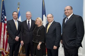
Above (right to left): Consul General Ido Aharony, Prof’ Peretz Lavie, Joan and Irwin Jacobs, Prof’ Haim Gotsman. Photo credit: Jeff Weiner

Harvey Prize 2012

 Harvey Prize 2012IMG_5497.jpg

In the Field of Human Health

To Professor Eric S. Lander

Broad Institute of Harvard and MIT, Professor of Biology MIT and Professor of Systems Biology at Harvard Medical School.

In recognition of his significant contributions to the field of genomics, as the driving force behind most of the major advances in this field. He has made important contributions by both developing methods to exploit the power of genetic information and leading large endeavors to identify and annotate entire genomes. Most notably he consolidated the efforts of the human genome project and first-authored the resulting historic manuscript.  Prof. Lander also pioneered the analysis of the genetic components underlying complex diseases, including cancer.

Harvey Prize 2012

In the Field of Science and Technology15

To Professor Eli Yablonovitch

Professor of Electrical Engineering and Computer Science, University of California, Berkeley, USA

In recognition of his pioneering discoveries in the fields of photonics, optoelectronics, and semiconductors. His groundbreaking studies are highly influential and broad in scope, combining deep physical insights with an applied technological approach. He established the field of photonic crystals and photonic band gap engineering, made fundamental and pioneering contributions to the research and development of photovoltaic cells, and the design and improved performance of semiconductor lasers.

Israeli scientists develop first photonic topological insulators to provide protection for transport of light

Researchers at the Technion-Israel Institute of Technology have developed and successfully demonstrated a photonic topological insulator, a new device used to protect the transport of light through a unique, lattice of ‘waveguides’. The advancement may play a key role in the photonics industry. A description of the advancement was published in the current issue of NATURE.

The photonics industry is at the heart of modern computing and communication.  It has allowed vast amounts of data to be transmitted extremely quickly over fiber optic lines that cross the oceans.  Photonic technology (i.e., technology that is based on the flow and control of light) is at the heart of DVDs, fabrication of computer chips, and solar cells.

As computers get faster and computer chips get denser, there is a need for smaller and smaller devices that manipulate light.  But when devices get smaller, imperfections in the fabrication processes can play a large role, making light move irregularly and unpredictably.  In other words, there’s a need for a new methodology to prevent unwanted scattering from any kind of defect.

Researchers at group of Prof. Mordechai (Moti) Segev at the Technion, in collaboration with the group of Prof. Alex Szameit at the Friedrich-Schiller University in Jena, Germany, have done exactly that.  Using a lattice-work of ‘waveguides’ (which are like wires that guide light instead of electricity), the researchers have experimentally demonstrated a ‘photonic topological insulator.’  The researchers used an array of helical ‘waveguides’ (shaped like curly hairs) arranged in a ‘honeycomb’ lattice structure, similar to the pattern observed in beehives.  In such a structure, where each waveguide is thinner than a tenth of a human hair, light is ‘topologically protected,’ which means it flows uninterrupted despite the presence of defects.

According to Professor Segev, “topological protection means that light simply flows around imperfections essentially without noticing them.”

Topological protection was first conceived not for light, but for electrons flowing in a solid material.  However, Dr. Mikael Rechtsman and Mr. Yonatan Plotnik from the Technion, figured out how to bring topological protection into photonics, using an array of waveguides that interact with one another.  The additional step needed to achieve topological protection was to make the waveguides helical (in the shape of a helix), rather than straight.  “The helical nature of the waveguides breaks the symmetry, so that in the forward direction the waveguides are spinning clockwise, and in the backward direction, counterclockwise,“ said Dr. Rechtsman.  “In our procedure, this is an essential ingredient in preventing unwanted scattering.“

“Photonic topological insulators have the potential to provide an entirely new platform for probing and understanding topological protection,” explained Rechtsman. “For example, all sorts of experiments that would be difficult or impossible to carry out in solid-state materials can now be accessed using light.” “Also”, added Plotnik, “such new ideas might one day be an important part of the optical communication industry, being robust to scattering and disturbances: a super conductor of light”. “This discovery is another step in the progress towards optical and quantum computing” said Julia Zeuner, the graduate student at Friedrich-Schiller University in Jena, who fabricated the sophisticated photonic structure and did part of the experiments. Her contribution, as well as the contribution of her PhD advisor, Prof. Szameit, was absolutely crucial, and manifested a long standing Israeli-German collaboration between the teams.  “We have discovered a completely novel phenomena”, concluded Professor Segev, “and new phenomenon are destined to find applications in directions that we can’t even imagine”.

Cathy Dove, Vice President of the Technion-Cornell Campus in New York: The Applied-Engineering-Science Center for Research to open in 2017 will impact the entire city

13A delegation of 30 senior entrepreneurs and officials of NYC’s Department of Economic Development visited the Technion and met with economic leaders

“The joint Technion-Cornell research center will have a huge impact on New York City,” says Cathy Dove, the newly appointed Vice President of the Technion-Cornell Campus in New York, on her recent visit to Israel with a delegation of 30 senior entrepreneurs and officials of NYC’s Department of Economic Development.

“New York City Mayor Michael Bloomberg has made it a goal to develop the high-tech industry in the city and to attract companies, investors and technology entrepreneurs. The joint Technion-Cornell Applied-Engineering-Science Center for Research will play a pivotal role in achieving this end,” adds Dove, in charge of infrastructure development and operations, as well as human resources on the new campus. “Bloomberg envisions this project as a magnet for attracting high-tech companies and students in engineering and technology fields. The research center will change the face of the entire area and will have a huge impact on NYC, starting from developing the public transportation to the Roosevelt Island, necessary for the establishment of the campus, through the construction of residential towers for students and the academic faculty, and the creation of thousands of new jobs.”

Dove explained that places not on the subway lines are considered by New Yorkers to be inaccessible. According to her, developing the public transportation on the Island is necessary and a key to the progress of the new campus, and will occur simultaneously with the construction of the campus. The campus will be built in a number of stages, starting from the northern part of the Island southward, with its construction consistent with the progress of public transport development in the area.

Already in the initial stages of campus construction, scheduled to open in 2017, residential towers for students and academic faculty will be built alongside academic buildings, which will draw new residents to the area. “The new campus will create hundreds of new places of work, in construction and infrastructure, and in service oriented jobs on the new campus,” says Dove. “It is well known that the establishment of a university has a catalytic effect on urban development. The new research center will act as a stimulus for growth and prosperity of the entire region.”

Members of this sizeable delegation met at the Technion with Israel’s senior economic leaders. According to delegation, a “high-tech strip” has already formed in New York all along the “F” subway line. “We are seeing start-ups forming one next to the other in minutes, and as far as we can tell, the interactions between these companies are excellent.”

The panel was hosted by Dr. Yossi Vardi, who emphasized that Uzia Galil (present in the audience) and Dan Tolkovsky are hailed as  “the fathers of Israel’s high-tech industry.”  He added that the establishment of the Technion-Cornell campus in the middle of NYC is sure to draw serious investors and spur high tech growth in the region, just as development centers of multinational companies were built in Haifa near the Technion, the high-tech industry of the Silicon Valley grew near and around Stanford, technology centers were established along the 128 Highway running near MIT, and the British high-tech industry situated itself near the University of Cambridge.  Even the famous “Bell” laboratories were built near the University of Princeton.

All attendees were presented with the book “Technion Nation: The Technion’s Contribution to Israel and the World” by Professors Amnon Frenkel and Shlomo Maital.

Above: Cathy Dove with Technion’s President Professor Peretz Lavie

First ever comprehensive survey by American MIT and Russia’s Skolkovo findings: Technion is ranked 6th place for entrepreneurship and innovation in the world

And 1st place for supporting a “challenging environment” among universities worldwide

The Technion was ranked in sixth place in the world for entrepreneurship and innovation, in the first ever comprehensive survey conducted by the Massachusetts Institute of Technology (MIT). The study was performed in collaboration with Skolkovo (the Innovation Center known as Russia’s Silicon Valley). The survey aimed to identify the most innovative universities around the world.

Among the top ten leading universities worldwide – only two institutions of higher learning are located outside the United States and Europe – the Technion and the National University of Singapore (NUS). MIT and Stanford University topped the list.

The survey findings also showed that the Technion and Imperial College London are counted among the “emerging giants whose reputation had grown considerably in recent years.”

The study was carried out among 61 experts in 20 countries. They identified 120 universities having brought decisive influence and major contributions to the world in the areas of entrepreneurship and innovation. In answer to the question: Which universities would you identify as having created/supported the world’s most successful innovation ecosystems? – the Technion was ranked at sixth place, after MIT, Stanford, the University of Cambridge, Imperial Collage London, and the University of Oxford, and ahead of the University of San Diego, UC Berkeley, ETH Zurich, and NUS in Singapore. Owing to the Technion’s standing, Israel was ranked third in the areas of entrepreneurship and innovation, after the United States and Great Britain, and ahead of Sweden, Singapore, Germany, Switzerland, the Netherlands, China and Canada.

The Technion was ranked first place in answer to the question: Which universities would you identify as having created/supported highly effective technology innovation ecosystems despite a challenging environment? Ahead of universities in France, New Zealand, Finland, Great Britain, Korea, China, Russia and the United States. As a result, Israel was nominated to first place in this category.

Instituting an institutional E&I culture – for entrepreneurship and innovation – is considered among experts as the essential ingredient for sustaining a successful system. In this respect, the Technion is mentioned as an institution that possesses the ethos of aspiration and achievement.

This is the first stage (out of three) in the comprehensive survey. In his reaction to these most favorable results, Technion President Professor Peretz Lavie said, “Technion’s position among the top ten leading universities in the world in the areas of innovation and entrepreneurship brings us closer to fulfilling our mission goals: to be counted among the top ten leading universities in the world. This is not the first time the Technion has earned international acclaim such as this,” he continued. “The university’s contribution to Israel’s advanced technology industry is recognized around the world. Not by coincidence did we prevail in the New York City’s tender last year to establish a scientific-engineering research center in partnership with Cornell University. The city’s mayor, Michael Bloomberg, said then that the Technion is the only university in the world capable of successfully turning the economic tide of an entire country, from exporters of citrus fruit to a global center for advanced industry and an authority of knowledge. To date, 61 experts from around the world have endorsed this statement.”

Professors Avram Hershko and Aaron Ciechanover, Technion Nobel Laureates, were elected to the American Association for Cancer Research (AACR) Academy for their exceptional scientific contributions

12The list of AACR Academy fellows represents the most distinguished group of scientists from around the world in biology and medicine in the second half of the 20th century and the beginning of the 21st century

Professors Avram Hershko and Aaron Ciechanover, Technion’s 2004 Nobel Laureates in Chemistry along with their colleague Professor Irwin A. Rose from the University of California in Irvine, were elected as fellows of the first class of the Academy of the American Association for Cancer Research(AACR).  This first class will be inaugurated during the upcoming annual conference of the AACR. The AACR Academy was established to recognize and honor scientists who have made substantial contributions that have propelled significant innovation and progress in the research and development of therapies against cancer. Fellows are selected through a rigorous process involving peer review, which evaluates them based on their scientific achievements in cancer research.  The Technion’s esteemed researchers and their colleague Rose were elected to the academy for “their breakthrough discoveries in the understanding of mechanisms of malignancies, which paved the way for development of novel effective drugs to treat them.”

“Our Board of Directors decided to found the AACR Academy as a means by which to recognize scientists whose contributions to the cancer field have had an extraordinary impact,” says Margaret Foti, Ph.D., M.D., chief executive officer of the AACR. “Membership in the Fellows of the AACR Academy will be the most prestigious honor bestowed by the American Association for Cancer Research.”

The inaugural class of AACR Academy fellows will consist of 106 individuals, a number that symbolizes the “age” of the organization upon the establishment of the Academy.

The list of fellows of AACR represents the most distinguished group of scientists from around the world in biology and medicine in the second half  of the 20th century and  the beginning of the 21st century. One of the most prominent scientists in this group is James Watson, who was among the discoverers of the double helix structure of DNA. The list includes many Nobel Laureates, among them Professor Paul Berg (Nobel Laureate in Chemistry 1980, for his fundamental studies of the biochemistry of nucleic acids, with particular regard to recombinant-DNA), Sydney Brenner who was awarded the 2002 Nobel Prize in Medicine or Physiology (with two other colleagues, H. Robert Horvitz and John E. Sulston for their discoveries concerning programmed cell death – apoptosis), Robert Lefkowitz (the 2012 Nobel Laureate in Chemistry, for his joint studies with his colleague Brian K. Kobilka of G-protein-coupled receptors), and Shinya Yamanaka (the 2012 Nobel Laureate in Medicine or Physiology; the prize was awarded jointly with his colleague Sir John B. Gurdon for the discovery that mature cells can be reprogrammed to become pluripotent).

Above: Professor Hershko (left) and Professor Ciechanover. Photo: Technion Spokesman

Technion President to Serve for a Second Term

11The Technion Senate reelected the President Professor Peretz Lavie, by an overwhelming majority (92 in favor, 2 against and 2 abstentions) for a second four-year presidential term. The decision was approved unanimously a couple of days ago, by the Managing Committee of the institute. The nomination must also be approved by the Board of Governors, which will convene in the month of June of this year.

During his first term as president (2009-2013), Professor Peretz Lavie set at the top of his objectives the issue of recruiting new faculty members, a university’s most important asset, as well as appropriating resources essential for settling them comfortably and smooth integration to the Technion. From the very beginning of his presidential term and until the end of it (in 2013), the Technion recruited 130 new faculty members, and the number of faculty will have grown from 533 members to 564.

The second objective of Professor Lavie was to change the learning environment on campus by revamping the Technion’s image from a “rigid” institute that is inconsiderate to the wellbeing of its student body. “We are now in the midst of a process to transform this image – I will point out a number of actions we took in order to get to this stage,” says Professor Lavie. “Firstly, we continued and expanded the program “A Good Start” whose goal was to ease the “shock” of first year study loads at the Technion, particularly by improving the teaching of mathematics. Secondly, in cooperation with the Student Association, we made significant steps towards improving services to students, such as greater transparency regarding examination marks, the introduction of regulations that enforce a maximum time period for marking exams and publicizing test results, as well as significantly more lenient examinations procedures that are considerate to students in reserve duty or involved in parenting. Additionally, we began to upgrade and renovate teaching facilities in most of the faculties, for the benefit of students. The program “Spirited Campus” encourages students to enrich and vary their leisure time on campus. Recently, an interactive map of the Technion campus was launched onto the university’s website, showing the wide range of events and possibilities for spending leisure time on campus.” Professor Lavie mentioned the “Yanai Awards” – an individual award given to faculty members for outstanding excellence in academic education, and for the establishment of the Graduate Student Village providing high standard accommodations to graduate students with families.

In Professor Lavie’s first term as Technion President, a substantial increase was recorded in the research funds and in revenue from intellectual property, from seven million US dollars in 2008, to 21 million dollars in 2012. To encourage the commercialization of intellectual property, an investment fund was established for Technion companies and a seed fund to finance research under the Nevet Program.

Professor Lavie emphasized the momentous honor the university received jointly with Cornell University, upon being chosen by the city of New York in an international challenge, to establish an institute of scientific research and applied engineering in the heart of Manhattan. According to the President, winning this challenge, which was entered by over 40 leading universities from the United States and around the world, focused the attention of the academic world on the Technion’s achievements.

The recruitment of excellent faculty members will remain at the forefront of Professor Lavie’s objectives in his second presidential term. “The quality of the Technion and its future status will be determined by, first and foremost, the quality of its faculty,” says Professor Lavie. The Technion President added that in the next four years he will continue to develop interdisciplinary research centers in addition to the establishment of centers of excellence awarded to the Technion in a national challenge by Israel’s Council for Higher Education. Additionally, development will continue with respect to the international activities on the Haifa campus. “For this reason we have created a new framework, “Technion International,” which unifies all of the Technion authorities responsible for and connected to international activities on campus,” he said. “In the next four years we will continue to work towards increasing the numbers of foreign post-doctoral and graduate students on campus, while meticulously adhering to ensuring their academic standing, in keeping with how this process has been done to date.”

At the Prime Minister’s Request: Technion Researchers Prepared the Gift for President Obama

The Declarations of Independence of the United States of America and the State of Israel, inscribed on a silicon chip affixed to a Jerusalem Stone dating to the Second Temple Period

As requested by Prime Minister Benjamin Netanyahu, scientists of the Technion’s Russell Berrie Nanotechnology Institute inscribed replicas of the Declarations of Independence of the United States of America and the State of Israel side-by-side on a gold-coated silicon chip, using a focused beam of high energy gallium ions. The area of the etched inscription is 0.04 square mm, and it is 20 nanometer, or 0.00002 mm, deep. The chip was affixed to a Jerusalem Stone dating to the Second Temple Period (1st century BCE to 1st century CE), such as the stones used to seal clay vessels. .

The etching was done by accelerating charged atoms, called ions, and bombarding them at various points on the surface of the chip. When an ion beam hits the chip it creates a tiny recess, in this case 20 nanometers deep. This is similar to digging tiny holes in the ground using a water jet out of an irrigation hose, except that the holes formed this way are a million times bigger than the holes created by the beam of ions.

The silicon chip is coated with a 20 nanometer thick gold film.  When the ion beam forms a hole 20 nanometers deep at a certain point on the surface of the chip, it sputters away the gold film, revealing the silicon beneath it. Scanning the chip with an electron microscope shows that the regions where the silicon was exposed are darker than the surrounding gold coated areas. Thus, any image can be transferred to the chip.

The preparation work for the etching took about a week. The image etched on the chip contains over two million dots. The ion beam was aimed at the required dots on the chip using a computer, so that the entire engraving process took less than an hour.

During the engraving the chip was part of a round silicon slice 5 centimeters in diameter and 0.13 millimeters thick. The chip was detached from the slice by chemically corroding the silicon slice around it with an advanced plasma tool.

The original image was translated into etching instructions using a special program developed for this purpose by Dr. Ohad Zohar, who conducted his Ph.D. under Prof. Uri Sivan of the Physics Department. The engraving was done by Dr. Tzipi Cohen-Hyams, in charge of the Focused Ion Beam lab in the Russel Berrie Nanotechnology Institute. The large team that took part in the work comprised Prof. Wayne D. Kaplan, Dean of the Department of Materials Science and Engineering; Prof. Nir Tessler, Head of the Center for Mircoelectronics and Nanoelectronics;  Mr. Yaacov Shneider, Chief Engineer in the Center of Mircoelectronics and Nanoelectronics; Dr. Orna Ternyak, Plasma Senior Engineer in the  Micro and Nanofabrication Unit and Ms. Svetlana Yoffis, process engineer in  the  Micro and Nanofabrication Unit.

10

The chip on the stone

Three Projects by Technion Researchers and Graduates to be Presented to President Barack Obama

Three projects by Technion Researchers and graduates to be presented to President Barack Obama during his visit to Israel.

Snake Robot

The robot was developed by Prof. Alon Wolf of the Faculty for Mechanical Engineering at the Technion. It is designed to enter spaces in areas prone to earthquakes and the collapse of buildings and to assist in location and rescue activities, by transmitting pictures and voices of trapped people. The robot is unique due to its crawling capabilities and is very flexible thanks to large number of links. Each link comprises engines, computer, sensors, wireless communication and batteries. The robot carries a camera in its head. Thanks to the snake’s flexible structure, it is capable of squeezing through the ruins without causing additional collapse of the structure, and is able to provide vital information from inaccessible areas about the condition of trapped people, the existence of hazardous  materials, etc.

ReWalk

Technion graduate Dr. Amit Goffer, founder of “Argo Medical Technologies”, will present the ReWalk, a powered external skeleton that enables  paraplegics to walk and perform other daily functions (sitting, standing,  and climbing/going down the stairs). The ReWalk is the first system of its kind. It is designed  to change the life of paraplegics, and Stephen Hawking  has defined it as one of the five most important machines for humanity. The device has already given almost 200  paraplegics the ability to walk , and  is used in the USA, Europe and Israel, including for partaking in Marathons. Amit will present the ReWalk, and Raddi Kaiuf,  paraplegic as a result of war injury, will demonstrate the system.

The system allows paraplegics to restore lower body function through a designated device that is harnessed to the body. The device is activated by a chargeable battery that lasts the entire day. The system uses motion sensors to identify the user’s movements and translate them to joint movements.

The users no longer need to use a wheelchair and they can move and stand upright. The ReWalk allows the user to walk on planes and slopes.

Generation of future scientists

Yarin Frenkel, Omer Zamir and Omer Shoshan, students at the Haifa Municipal High School C are the winners of an international robotics contest held in Connecticut, USA, in 2012. The students, guided by Prof. Igor Verner and his doctoral candidate Dan Cooperman, of the Department of Education in  Technology and Science at the Technion, have won for their development of a waiter robot that is aimed at demonstrating the ability to serve the  handicapped in their home. They  developed a “human” waiter  robot, which is better accepted by the user. The robot has 18 engines, sensors, a compass and a camera.

From right to left: Yarin Frenkel, Omer Shuham and Omer Zamir

Photos: Technion Spokesman

Can thermal radiation exceed the limit Planck established more than 100 years ago?

We conceive the Sun as bright-white source of radiation and only the rainbow, is an everyday indication of the colors its light contains. A quantitative description of the colors emitted by a body held at a given temperature  was first developed by Max Planck in the early days of the previous century, relating the intensity of each color (wavelength) to the temperature of the body – provided the typical dimension of the body is significantly larger than the radiation’s wavelength.  Since inherently Planck’s formula is independent of the characteristics of the material, it is conceived to describe the upper limit to what a body can emit at a given temperature.  In the framework of an article published in PRA we have demonstrated that if the characteristic length of the emitting body is of the order of the wavelength, the intensity it emits, in a narrow range of wavelengths, may exceed significantly the prediction of Planck’s theory.  Such an enhancement may be designed to overlap the spectral region where a photo-voltaic cell performs the best, improving in the process its theoretical efficiency dramatically.

Navigating through mega malls & large buildings made simple: Students from the Technion developed a novel mobile indoor navigational system

5
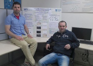
Winning project of the 2012 Amdocs Best Project Contest in collaboration with Qualcomm experts, this indoor navigation system helps you find your way within any large building using your “Smartphone”

Technion students from the Faculty of Computer Science developed a new indoor navigation approach, which enables you to locate your position and find your way around a large building with the help of your “Smartphone.” It was the winning project of the 2012 Amdocs Best Project Contest.

Students Alex Portnov and Dror Baum, supervised by Itai Dabran, Chief Engineer of Technion’s Laboratory of Computer Communication and Networking, and Constantine Elster from Qualcomm, built an indoor map screening and route finding system on a Smartphone that lets the user locate a store in a huge mall, find an office in a large office building, or get to a specific gate at an airport. The mobile system automatically sketches an efficient route to follow, to reach your destination point.

The application operates through multiple pathfinding stages:

  1. With the assistance of a Smartphone’s camera, the user photographs a printed or hand-written floor plan, area or maze.
  2. The phone sends the diagram to a server, which stores the picture together with additional parameters.
  3. The user indicates with his/her finger both the starting and destination points, and the phone sends a request to the server. The server initiates graphic algorithms and displays on the screen a drawing of the shortest distance between the two points that are obstacle free.
  4. The picture becomes stored in the server, and is given a QR Code so that it may be reused multiple times.

The algorithms are calculated very fast, and the map and route are drawn in under a minute.

“In effect, we built a framework for indoor map making and navigation, based on a building’s architectural plan,” explain Dror and Alex. “If a shopping mall’s floor plan will be featured in the form of a barcode at the entrance, shoppers will be able to scan it on their Smartphone and within seconds, get the shortest route to their desired store location.”

During the process, distractions such as colors are automatically eliminated from the scanned diagram, so that a clear navigational map can be achieved, upon which routes can be found and drawn.

Above: Dror (on the right) and Alex, with a poster describing their work. Photographed by: Itai Dovran, from the Technion

Nature Communications reports: Technion Scientists Develop a New Approach for Artificial Stimulation of Blind Retinas

4Method is based on optogenetics – a newly developing area in neuroscience, and is a first step towards non-invasive sight restoration in cases of degenerative retinal diseases

Scientists from the Faculty of Biomedical Engineering at the Technion developed a novel approach towards non-invasive vision restoration in blind retinas, by combining holography and optogenetics – a rapidly developing field in neuroscience. The study is published in the multidisciplinary Journal, Nature Communications.   

“Degenerative diseases of the outer retina are one of the major causes of blindness in the Western world,” says Professor Shy Shoham. “These diseases are characterized by degeneration of the photoreceptors, which serve as light sensors, while downstream cellular levels in the retina, and specifically the retinal ganglion cells, are relatively well preserved. Artificial stimulation of these neurons constitutes a potential strategy for getting around the damaged retinal nerve cells.  Restoring lost vision to basic functionality levels has become possible recently through invasive surgical insertion of artificial electronic implants that electrically stimulate surviving retina cells, similar to the snail-shaped cochlear implants used to treat the hearing impaired. Our approach is different and attempts to stimulate the surviving retinal cells without the need for direct implants onto the retina, and may eventually make surgery and implants redundant.”

“Our optogenetic approach relies on genetic expression of ion channels that are light sensitive (proteins derived from algae) in the ganglion cells of the retina,” explains Dr. Inna Reutsky-Gefen, who studied the combination of holography and optogenetics and its application to blind retinas during her doctoral thesis under the mentoring of Professor Shoham, and with assistance from additional study co-authors Lior Golan, Dr. Nairouz Farah, Adi Schejter, Limor Tsur, and Dr. Inbar Brosh. “The ganglion cells are natively transparent and not light-responsive, but after expressing the channel, transform into light-sensors and may be capable of substituting the function of the photoreceptors. In order to create a coherent visual perception in the brain, we have to be able to activate a large number of neurons simultaneously, just as it works in normal visual processing. In addition, this needs to be achieved with high temporal and spatial precision in order to imitate normal retinal information processing. Our study findings demonstrate that optical stimulation of these cells, with the use of a unique holographic projector, enables simultaneous stimulation of a large group of cells with spatial precision at the level of single retinal cells, which is not possible with electrical stimulation. In this manner we demonstrated, in principle, the first ever holographic photo-stimulation capable of restoring cellular activity similar to intact retinal behavior, as a basis for sight rehabilitation developments.”

The holographic projection method developed in the study uses diffractive spatial light modulation to generate images at the focal plane. This approach is light-efficient and does not ”throw away” much of the light energy. The researchers emphasize that this efficiency will be particularly useful in more advanced phases, where it will be required to miniaturize the system into a portable component of a retinal “prosthetic” system.

“Applications of this approach are not limited to vision restoration,” stresses Professor Shoham. “holographic stimulation strategies can permit flexible control of the activity of large cellular networks which artificially express light-sensitive channels, and pave the way towards new medical devices and scientific tools that can help “break” the brain’s neural code.”

The research was funded by a European Research Council Starting Grant to Prof. Shoham.

Illustration: Conceptual design of a future holographic retinal prosthesis mounted on a pair of glasses. Visual input from miniature video camera/s is converted in real-time into activation laser holograms projected onto genetically photo-sensitized retinal cells (in the back of the eye. Credit: Inna Gefen, Roman Kanevsky and Shy Shoham