
From the Terminator to Spiderman’s suit, self-repairing robots and devices abound in sci-fi movies. In reality, though, wear and tear reduce the effectiveness of electronic devices until they need to be replaced. What if the cracked screen of your mobile phone could heal itself overnight? Or, if the solar panels providing energy to satellites could self-repair the damage caused by micro-meteorites?
The field of self-repairing materials is rapidly expanding, and what used to be science fiction might soon become reality, thanks to Technion – Israel Institute of Technology scientists who developed eco-friendly nanocrystal semiconductors capable of self-healing. Their findings, recently published in Advanced Functional Materials, describe the process in which a group of materials called double perovskites display self-healing properties after being damaged by the radiation of an electron beam. The perovskites, first discovered in 1839, have recently garnered scientists’ attention due to unique electro-optical characteristics that make them highly efficient in energy conversion, despite inexpensive production. A special effort has been put into the use of lead-based perovskites in highly efficient solar cells.
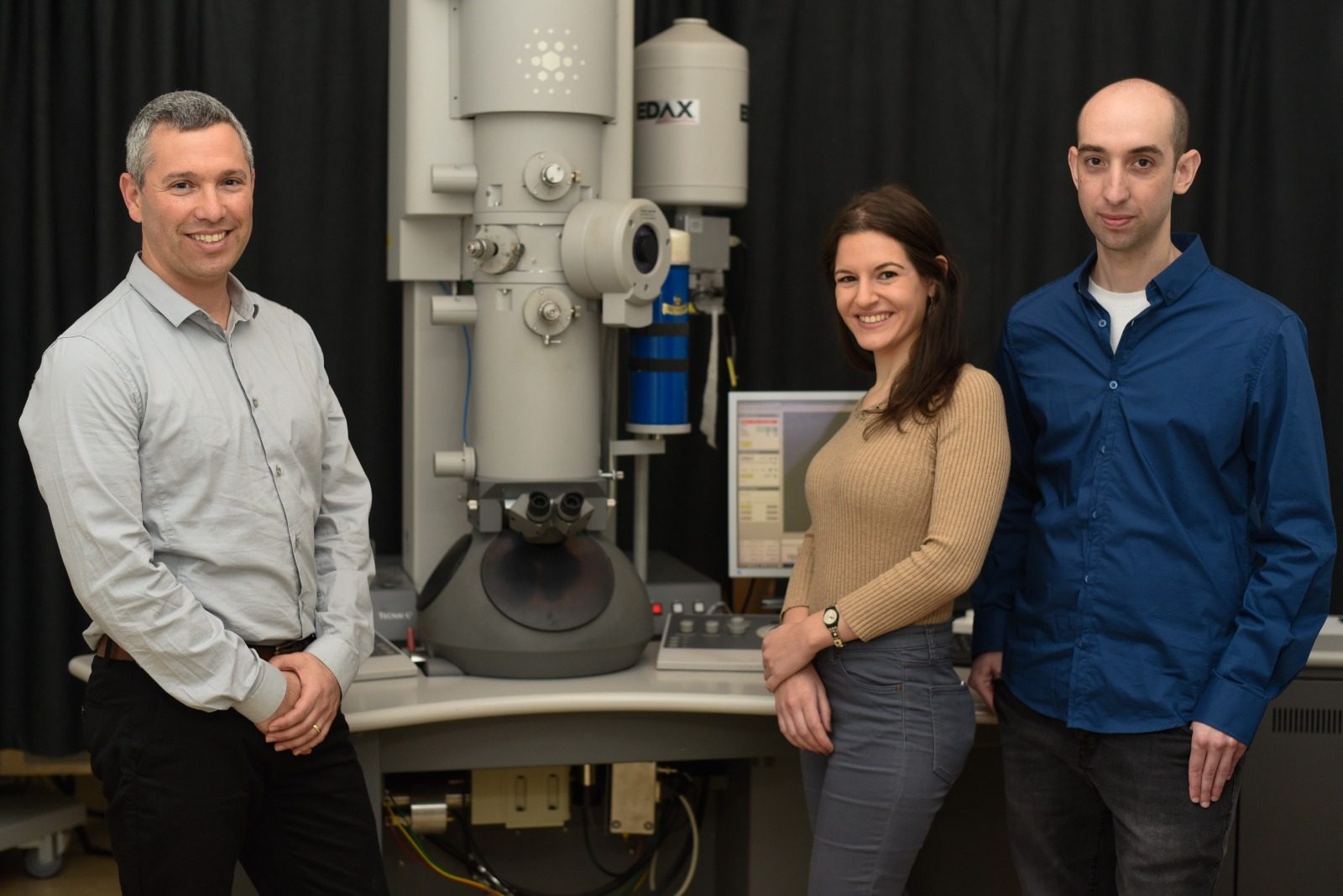
The Technion research group of Prof. Yehonadav Bekenstein from the Faculty of Materials Sciences and Engineering and the Solid-State Institute at the Technion is searching for green alternatives to the toxic lead and is engineering lead-free perovskites. The team specializes in the synthesis of nano-scale crystals of new materials. By controlling the crystals’ composition, shape, and size, they change the material’s physical properties.
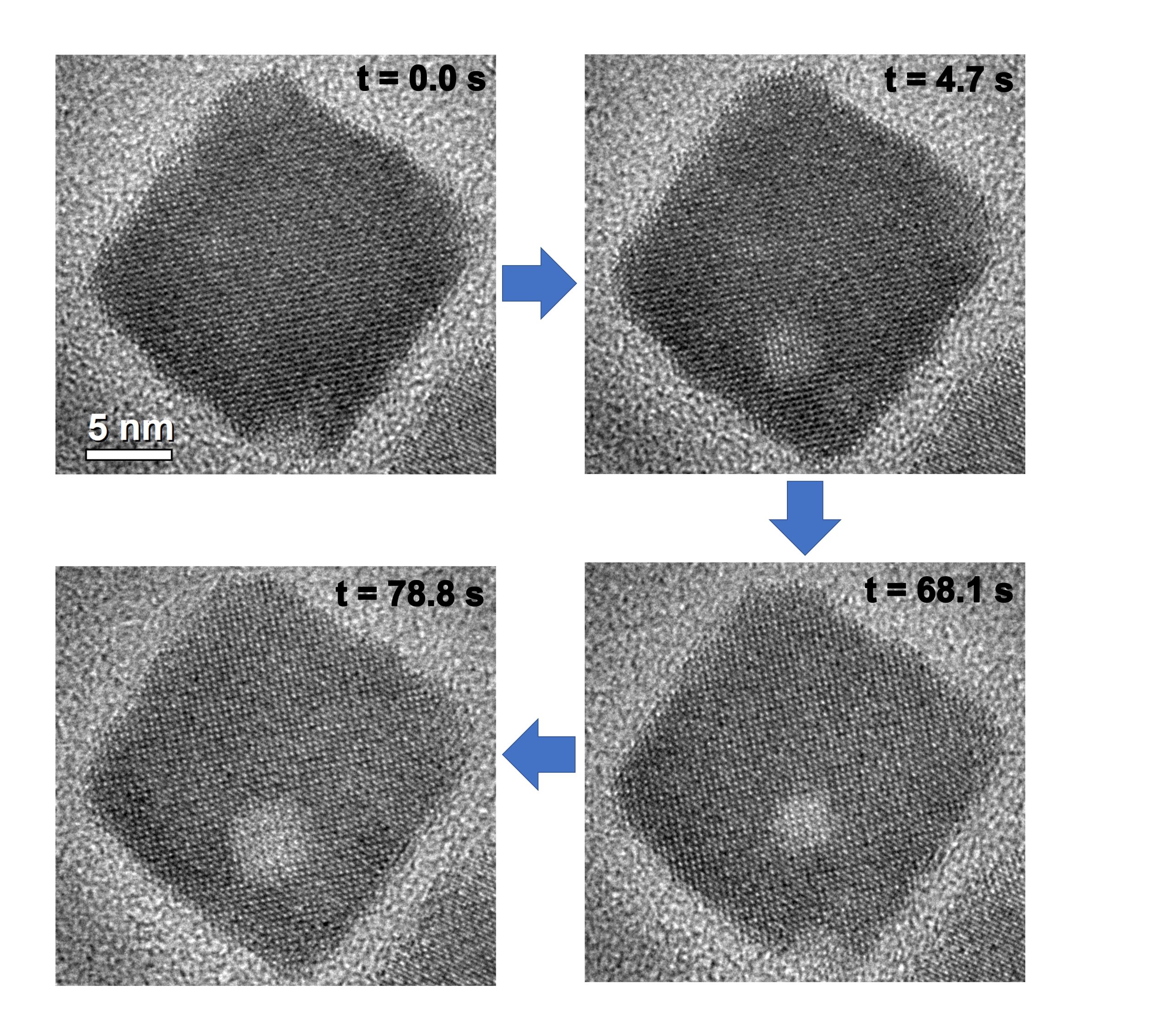
Nanocrystals are the smallest material particles that remain naturally stable. Their size makes certain properties more pronounced and enables research approaches that would be impossible on larger crystals, such as imaging using electron microscopy to see how atoms in the materials move. This was, in fact, the method that enabled the discovery of self-repair in the lead-free perovskites.
The perovskite nanoparticles were produced in Prof. Bekenstein’s lab using a short, simple process that involves heating the material to 100°C for a few minutes. When Ph.D. students Sasha Khalfin and Noam Veber examined the particles using a transmission electron microscope, they discovered the exciting phenomenon. The high-voltage electron beam used by this type of microscope caused faults and holes in the nanocrystals. The researchers were then able to explore how these holes interact with the material surrounding them and how they move and transform within it.
They saw that the holes moved freely within the nanocrystal but avoided its edges. The researchers developed a code that analyzed dozens of videos made using the electron microscope to understand the movement dynamics within the crystal. They found that holes formed on the surface of the nanoparticles, and then moved to energetically stable areas inside. The reason for the holes’ movement inwards was hypothesized to be organic molecules coating the nanocrystals’ surface. Once these organic molecules were removed, the group discovered the crystal spontaneously ejected the holes to the surface and out, returning to its original pristine structure – in other words, the crustal repaired itself.
This discovery is an important step towards understanding the processes that enable perovskite nanoparticles to heal themselves and paves the way to their incorporation in solar panels and other electronic devices.
Prof. Yehonadav Bekenstein completed his degrees in physics and chemistry at the Hebrew University of Jerusalem. Following a postdoctoral fellowship at the University of California, Berkeley, he joined the Technion faculty in 2018. He has received multiple awards, including the Käte and Franz Wiener Prize (Excellent PhD Thesis Award), the Rothschild Fellowship for postdoctoral scholars, and the Alon Scholarship for the Integration of Outstanding Faculty. In 2020 he was awarded the ERC Starting Grant for early-career scientists.
For the article in Advanced Functional Materials click here
Electron microscopy video displaying the formation of the hole on the surface of the nanocrystal and its movement inwards: