
Researchers at the Technion – Israel Institute of Technology have developed a new light source based on a single atomic layer. The discovery is based on the interaction of a single atomic layer with nano-antenna arrays in a silicon chip by creating defects in photonic crystals. Published in the journal Nature Nanotechnology, the development enables the control of the spin of emitted photons from two-dimensional matter and paves the way for new photonic devices based on “atomic scale spin-optics.”
The study was conducted in the research group of Professor Erez Hasman, head of the Atomic-Scale Photonics Laboratory, in collaboration with Professor Elad Koren, head of the Laboratory for Nanoscale Electronic Materials and Devices in the Department of Materials Science and Engineering. Both groups are associated with the Helen Diller Quantum Center and Russell Berrie Nanotechnology Institute. Dr. Kexiu Rong and Dr. Bo Wang conducted and led the research, and collaborated with Dr. Elhanan Magid, Dr. Vladimir Kleiner, Avi Reuven, Bar Cohn, and Shaul Katznelson.
What are two-dimensional materials? According to Prof. Koren, “In 2004, the possibility of creating a single atomic layer was first examined when physicists Andre Geim and Konstantin Novoselov, later Nobel Laureates in Physics (2010), developed a simple method for creating individual layers of carbon atoms. The two attached adhesive paper to a piece of graphite and peeled the material layer by layer until a single layer of atoms called graphene was obtained. They also showed that the atomic layer of matter is very different in its properties from the properties of matter in its three-dimensional form. This is a material 100 times stronger than steel and with exceptional electrical properties, and according to estimates it is expected to revolutionize conductors and semiconductors, monitors and screens, solar cells, and more. Following this discovery, atomic layers were developed from other materials, and they similarly exhibit surprising and unique properties.”

Professor Hasman added and elucidated that, “As a result of the discovery of graphene, many two-dimensional materials have been discovered and studied, such as various semiconductors that make it possible to obtain interesting optical properties. Standard electronic chips are based on silicon, which severely limits the development of the next generation of computers that require a combination of electronics and photonics, partly due to a lack of an essential condition called ‘direct energy gap’ in silicon. To our surprise, direct energy gap was discovered in two-dimensional semiconductors, which makes it possible to combine photonics and electronics at the nanometric scale, use them to produce light sources and active photonic devices, and pave the way for future generations of chips.”
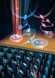
To miniaturize the electronic chip and significantly increase the processing speed and information transfer rate, the currently accepted approach is spintronics – performing operations on a spin, an important property characterizing the intrinsic rotation of electrons – and not on the current of electrons. In 2001, Prof. Hasman established a new field called spin-optics, which makes it possible to utilize the spin of photons using meta-surfaces for the purpose of transmitting and processing information in photonic chips. The transfer of information is based on the control of photonic spin with the help of nano photonics, optics at the nanometer scale. The semiconductor materials, due to the broken inversion symmetry of their structures, possess electron energy levels, characterized by a new degree of freedom – valley – that can control spin-selective light emission. Technion researchers decided to take advantage of this feature, creating an interaction of a single atomic layer of Tungsten Selenide (WSe2) with nano antennas that allow symmetry in the photonic spin to be broken. This will result in an atomic scale chip that controls and processes valley information via the photonic spin.

The researchers developed a two-dimensional photonic crystal structure made of silicon that creates an energy gap in the emission spectrum of the two-dimensional material so that the coupling of the atomic semiconductor to the photonic crystal blocks all optical emission channels from the two-dimensional material. By creating smart defects within the photonic crystal, controlling the phase of the defects with their geometry, and coupling between them, the researchers created a light source from a single atomic layer that separates and sorts the spins of the photons emitted from the two-dimensional semiconductor. This discovery will make it possible to combine spintronics and spin-optics to develop a wide range of devices on an atomic scale.
Prof. Hasman proudly noted that: “this prestigious publication shows the importance of multidisciplinary research that combines physics, chemistry, materials science, and engineering.”
The research was supported by the Israel Science Foundation (ISF), the Israel Ministry of Science, Technology and Space, the U.S. Air Force Office of Scientific Research and, in part, by the Technion via an Aly Kaufman Fellowship. The fabrication was performed at the Micro-Nano Fabrication & Printing Unit (MNF&PU) of the Technion.
Laboratory sites: https://hasman.technion.ac.il/ https://koren.net.technion.ac.il/
Click here for the paper in Nature Nanotechnology