At the Prime Minister’s Request: Technion Researchers Prepared the Gift for President Obama
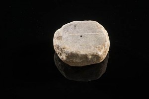
The Declarations of Independence of the United States of America and the State of Israel, inscribed on a silicon chip affixed to a Jerusalem Stone dating to the Second Temple Period
As requested by Prime Minister Benjamin Netanyahu, scientists of the Technion’s Russell Berrie Nanotechnology Institute inscribed replicas of the Declarations of Independence of the United States of America and the State of Israel side-by-side on a gold-coated silicon chip, using a focused beam of high energy gallium ions. The area of the etched inscription is 0.04 square mm, and it is 20 nanometer, or 0.00002 mm, deep. The chip was affixed to a Jerusalem Stone dating to the Second Temple Period (1st century BCE to 1st century CE), such as the stones used to seal clay vessels. .
The etching was done by accelerating charged atoms, called ions, and bombarding them at various points on the surface of the chip. When an ion beam hits the chip it creates a tiny recess, in this case 20 nanometers deep. This is similar to digging tiny holes in the ground using a water jet out of an irrigation hose, except that the holes formed this way are a million times bigger than the holes created by the beam of ions.
The silicon chip is coated with a 20 nanometer thick gold film. When the ion beam forms a hole 20 nanometers deep at a certain point on the surface of the chip, it sputters away the gold film, revealing the silicon beneath it. Scanning the chip with an electron microscope shows that the regions where the silicon was exposed are darker than the surrounding gold coated areas. Thus, any image can be transferred to the chip.
The preparation work for the etching took about a week. The image etched on the chip contains over two million dots. The ion beam was aimed at the required dots on the chip using a computer, so that the entire engraving process took less than an hour.
During the engraving the chip was part of a round silicon slice 5 centimeters in diameter and 0.13 millimeters thick. The chip was detached from the slice by chemically corroding the silicon slice around it with an advanced plasma tool.
The original image was translated into etching instructions using a special program developed for this purpose by Dr. Ohad Zohar, who conducted his Ph.D. under Prof. Uri Sivan of the Physics Department. The engraving was done by Dr. Tzipi Cohen-Hyams, in charge of the Focused Ion Beam lab in the Russel Berrie Nanotechnology Institute. The large team that took part in the work comprised Prof. Wayne D. Kaplan, Dean of the Department of Materials Science and Engineering; Prof. Nir Tessler, Head of the Center for Mircoelectronics and Nanoelectronics; Mr. Yaacov Shneider, Chief Engineer in the Center of Mircoelectronics and Nanoelectronics; Dr. Orna Ternyak, Plasma Senior Engineer in the Micro and Nanofabrication Unit and Ms. Svetlana Yoffis, process engineer in the Micro and Nanofabrication Unit.